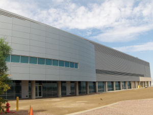
Intel 300 mm, 45 nm Facility Opens in Arizona
 The second of four production facilities for Intel's 45 nm semiconductors is now online, with the opening of the company's entirely new Fab 32 in Chandler, Arizona. Built specifically to use the company's breakthrough HK+MG manufacturing process that miniaturized the transistor all over again, Fab 32 represents the beginning of the big payoff of Intel's restructuring, establishing what it hopes to be a substantial and permanent "generation gap" between its CPUs and AMD's.
The building's million-plus square feet of space includes 184,000 square feet of dedicated clean room. By comparison, the company's D1D 45 nm facility in Oregon contains 176,000 square feet of clean room, and AMD's Fab 30 facility in Dresden, Germany is said to contain 120,000 square feet. There are two more 45 nm facilities under construction for Intel, including the colossal Fab 28 facility in Kiryat Gat, Israel, which will house over 200,000 square feet of clean room.
What does Intel mean by "clean?" In a "Class 1" facility such as Fab 32's, there should be no more than one loose particle measuring half a micron or larger swirling around in the average cubic foot of air. That's 100 times cleaner than a hospital operating room, by Intel's estimate, and a million times cleaner than the space around my desk.
But Intel is saying Fab 32 plans to be relatively clean on the outside as well. Already, the company's Ocotillo production facility outside Chandler, where its existing Fab 12 and Fab 22 are stationed, was able to recycle and reuse 79% of its water and 74% of its solid waste - a full 57,000 tons worth - throughout 2006. For that reason, among others, Intel is seeking what's called LEED status (Leadership in Energy and Environmental Design) for Fab 32. That's a certification granted to factories and other facilities by the US Green Buildings Council.
"LEED promotes a whole-building approach to sustainability by recognizing performance in five key areas of human and environmental health," reads the USGBC's Web site, "sustainable site development, water savings, energy efficiency, materials selection, and indoor environmental quality."
With all the attention being paid to Intel's newest facilities, what exactly will happen to the older ones? The Arizona Republic was concerned the company could close Fab 12, as it did recently with Fab 11 in Albuquerque, New Mexico. But Intel spokesperson Chuck Mulloy told the paper last week Intel has no plans to close Fab 12, and could actually upgrade it. The Chandler/Ocotillo campus already employs about 10,000, and 1,000 of those will be assigned to Fab 32.
| Semiconductor manufacturers are typically very reluctant to show the interior of their factory floors, because not only are their products protected by patents, but their manufacturing process as well. So this is about as far "inside" Fab 32 as many will ever see, and if you ever get deeper yourself, you won't be bringing a camera.
This is just a corridor toward the exit, most likely along the perimeter of the complex. But running along the top rails, making their way from stage to stage along with the technicians, are the FOUPs - front-opening unified pods, which contain the 300 mm wafers from station to station as they're etched, verified, and refinished. Those FOUPs are the "hands" that hold and protect the wafers, lowering them into position all the way down from the ceiling to eye-level, but at the same time keeping them from being touched even by relatively clean, covered hands. (Courtesy Intel) |